MOSIS, short for Metal Oxide Semiconductor Implementation Service, is to integrated circuits what BatchPCB is to printed circuit boards. That is, it’s a batch order service that makes getting your own custom ICs fabricated more affordable by allowing lots of designers to contribute their designs and share the costs of a single IC fabrication run.
The difference in this case is that unlike your typical PCB pool, where a single board might cost $20, in IC-land, “affordable” means “tens of thousands of dollars’.” For this reason, MOSIS is usually reserved for use by universities and startup companies, not by individuals.
However, that doesn’t mean that some particularly ambitious people haven’t used MOSIS to make their own chips before.
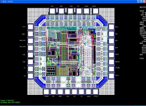
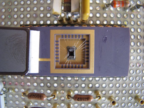
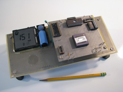
The photos that follow and the chip layout shown above are one example of an individual, Scot Satre of Satre Electronics, who in 2004 decided to design some of his own application-specific integreated circuits (see ASIC) in his spare-time.
I’m sure there have been others, but this is surely one of only a few examples of an individual having their own custom chips made.
I find this sort of thing very inspiring. Will there be a time when individuals can submit their own chip designs to a multi-project wafer (MPW) like we submit PCB designs to group orders today?
Gold Phoenix makes BatchPCB possible by providing cheap offshore PCB fabrication services. Where is the Gold Phoenix of semiconductor foundries that will make DIY IC design affordable for ordinary people and not just universities, corporations, and VC-funded startups? Where are the free, open source tools that will enable you and I to simulate and layout our own chips?
If you could design your own integrated circuit, what would you make?
Photos: Scott Satre / Satre Electronics


I would make a ternary IC (with true balanced ternary where each signal could be not only 1 and 0, but also -1)
I’d use it to make a multi-core pipelined SHA256 calculation device. A large-ish FPGA can barely fit one such pipelined core, allowing for something like 200 million 1-block hashes per second – which is approximately the hashing speed that a good graphics card can manage via OpenCL. An ASIC would allow the core to run significantly faster, and extra cores can be packed in a relatively small size.
Why? For cracking SHA256 of course!
Good post. As an RF IC Designer I know that for RF IC designs DIY is like an utopia. Higher frequencies demands IC fabrication process that are very expensive even for enterprises. For example, a 2.4GHz IC design may demand a tapeout that costs more than $ 100k at MOSIS. But is a good option for designs made at University, with MEP (MOSIS Educational Program) that for course projects is free of charge in technology of 0.5um (that allow designs up to 1GHz).
Would be interesting alright. But as mentioned, the cost of making the litho masks is the big up-front cost.
But what kind of projects would you want your own ASIC for? I understand that it would be nice to do for the sake of it, but: custom analog designs may need lots of revs to get right, and if you just want to pack loads of digital in, then maybe an FGPA is the way forward.
Marty,
I agree that for most digital designs, FPGA is the way to go. I have never done any FPGA development, but my understanding is that you can fairly straightforwardly create an entire CPU core on an FPGA if needed, so that certainly makes sense given the costs of custom IC development.
That’s why I ended the post with a question – if you had this capability, what would you make with it? What is not available off the shelf or can’t be built with existing programmable logic devices?
Analog and RF circuits are certainly good candidates. But then you are into the territory of multiple spins (for RF, many!) and expensive proprietary simulation tools.
I agree that “just because” may not be sufficient reason to make your own integrated circuits, but then again, if you lower the barrier to entry and make the technology available to lots of creative people, who knows what could come out of it…
I would duplicate the project I did as a Caltech undergrad; no, I would do it right this time! It was a chip that executes the “unification” algorithm from Automated Theorem Proving (specifically, Robinson’s resolution proof). The problem definition had a problem, because a prof told me to design a chip that can attach to an IBM PC and “take over the bus,” yet as far as I can tell there is no way to tell the CPU to stop sending any signals to the bus (to let the bus wires “float” unconnected to either power or ground, so that I can connect them to power or ground as I desire). And thus it is impossible for an add-on chip to take over the bus. However, I am more recently told that Firewire is amenable to that.
Might look at this: http://www.physics.rutgers.edu/ugrad/387/388s06/film_deposition/Musgraves05.pdf
About $5000 for a DIY DLP photolithography setup capable of doing ICs. That could be another way to go, as my understanding is a lot of the cost of IC fabrication is mask costs, and DLP would go maskless.
Yes, but there is still lots of processing before you have a finished IC. And that processing involves equipment and chemicals which are not very compatible with home fabrication, unless you are Jeri.
(For those who haven’t seen Jeri’s DIY chip fab work before, check out http://www.youtube.com/watch?v=w_znRopGtbE&feature=related)