
Here’s a really cool Instructable about using a flexible copper-clad material called Pyralux to make flexible printed circuit boards. You could make some really cool business cards with this stuff.
(via makezine)
Here’s a really cool Instructable about using a flexible copper-clad material called Pyralux to make flexible printed circuit boards. You could make some really cool business cards with this stuff.
(via makezine)
As I wait for my AVR High Voltage Programmer Shield PCBs to come back from BatchPCB, I’m starting to wonder what prototype PCB services other people are using for their boards.
Ladyada has a PCB Cost Comparison Calculator that shows the significant differences in price between various low volume PCB vendors, but what’s missing from the chart is the answer to: What vendors are people actually using?
If the cheapest fab house is also the best, obviously the more expensive vendors wouldn’t be around, would they? Unfortunately, it’s usually not that simple, cheap usually means slow, or low quality, or both.
I know that some visitors to this site make prototype PCBs at home and others send them out to be fabricated. How do you get your prototype boards made? Vote below.
[poll id=”2″]
Soldering surface mount (SMT) components is tricky, particularly if you can’t see what you are doing due to the small scale of most SMT parts. Since I started working with SMTs at home I have suffered with a 10x magnifier ring-light. It works, but it’s tricky to use, mainly because the working distance is so small that getting a soldering iron on a part and keeping that part in focus are almost mutually exclusive.
The right tool for this job is a stereo microscope. Stereo microscopes use two separate optical paths to provide you with depth perception, very helpful for working with 3-dimensional objects like printed circuit boards. Even better is a stereo zoom microscope, where the magnification factor can be changed by turning a knob instead of swapping out lenses.
Until now I assumed that a stereo zoom microscope would be way out of my price range, at least several hundred or a thousand dollars for a very basic setup. However, some searching on eBay showed that good deals can be had, and a used microscope with a boom stand suitable for surface mount work can be found for as little as $200-$300. New microscopes are available for $400-$500, although there is some debate regarding the quality of low-cost imported microscopes. Caveat emptor.
For surface mount soldering, 7-30x magnification is reasonable (that’s 10x eyepieces * a 0.7-3x objective), and a 4″ or greater working distance makes using tools under the microscope a lot easier.
I ended up buying an American Optical (AO) model 569 with an illuminator and boom stand, shown below. Total cost was just over $200 with shipping.
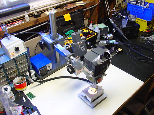
Combined with the PID controlled hotplate I just put together this is a very powerful setup for doing rework of very tiny components – I could probably work with 0402’s, maybe even 0201’s if I was careful. Using this setup, 0805’s are easy. (and they look huge!)
The scope is very old, it was made in the late 1970s, but it has survived in extremely good condition. Upon receiving it, I tightened some setscrews and regreased the slides and it’s as good as new, despite being over 30 years old!

There are a few more photos of the microscope setup on flickr.
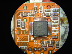
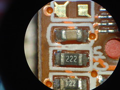
The image quality is excellent. Here are a couple pictures of my SYBA USB-Audio Adapter taken with the microscope and my Sony DSC-V1 digital camera. I held the camera up to one eyepiece, set it into macro mode, and snapped the shutter – these images are straight off the camera with no retouching.
When you finish a PCB design, you typically use the CAM export function of your layout tool to generate a set of gerber files to send to the PCB manufacturer. To avoid errors in the finished board, it’s usually a good idea to review the files before you click send.
Enter gerbv, a free, open source gerber viewer that is available for many platforms, including Debian and OS X (via fink).
I recently upgraded to version 2.0 (I was using the really outdated version 1.0 on Macports) and I am really impressed by the improvements in the GUI and overall usability.
gerbv is a part of the gEDA suite, which also includes layout and schematic capture tools that are slowly becoming more popular vs. more established non-free tools like Eagle.
Update: I missed an interesting update to a post over on My 2uf, not everyone seems to like the rest of the gEDA suite.


What’s this???
In response to the continued demand for a PCB version of my Arduino-based AVR High Voltage Programmer, I just released a first cut to BatchPCB and should have a prototype within 3-4 weeks.
This design is an improvement upon the original HV programmer shield in the following areas:
I hope to have kits for sale in early February. Sorry for the delay in getting these made, but I wanted to make the best possible shield I could!